
发布日期:2026/03/24来源:

In March 2026, Hangzhou Garen Semiconductor Co., Ltd. (hereinafter referred to as "GAREN SEMI") made a major technological breakthrough in epitaxy technology, successfully realizing high-quality 8-inch gallium oxide homoepitaxial growth for the first time worldwide. The test results of the epitaxial wafer show that: the epitaxial film thickness is > 10 μm with a thickness variance σ < 1%; the average carrier concentration of the epitaxial layer is 1.79×10¹⁶ cm⁻³.
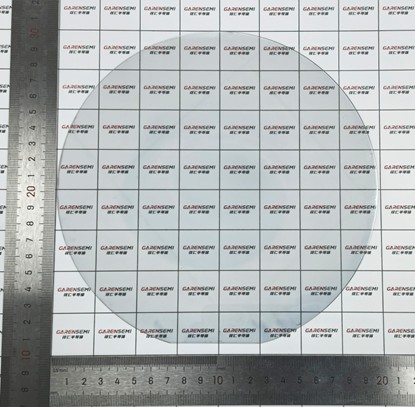
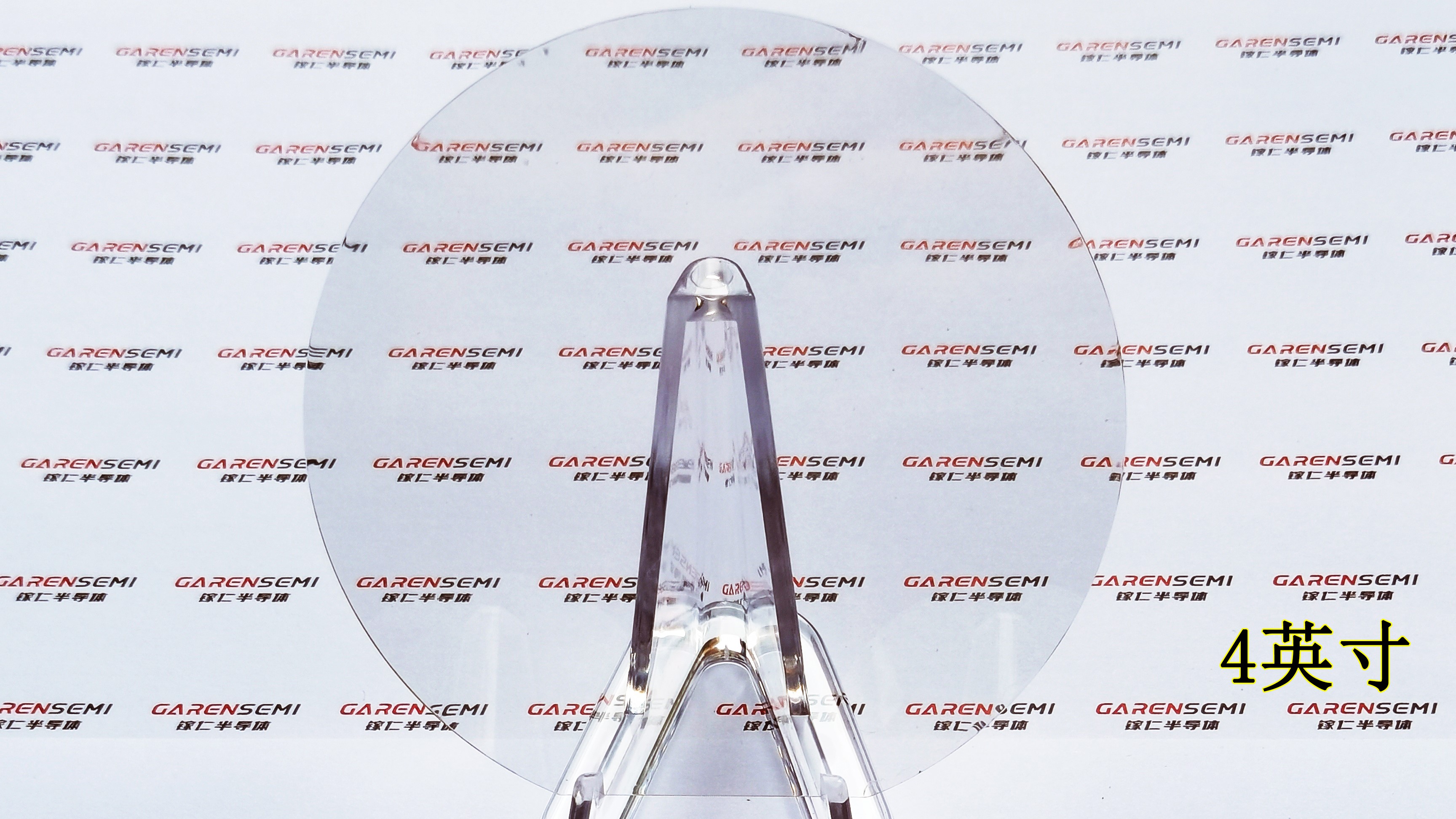
Fig.1 GAREN SEMI 8-inch Gallium Oxide Homoepitaxial Wafer
Film thickness testing shows that the 8-inch gallium oxide epitaxial wafer has an average thickness of 13.05 μm with excellent thickness uniformity and a variation of merely σ=0.58%. This data fully attests to the superior controllability and consistency of GAREN SEMI's epitaxial growth process. For power electronic devices, high voltage withstand capability is a core performance attribute, and the epitaxial layer typically serves as the drift region—the primary area responsible for the device's voltage blocking capability. Notably, the thickness of the drift region is positively correlated with the device's breakdown voltage, making a thick, highly uniform epitaxial layer a fundamental guarantee for manufacturing high-performance high-voltage power devices.
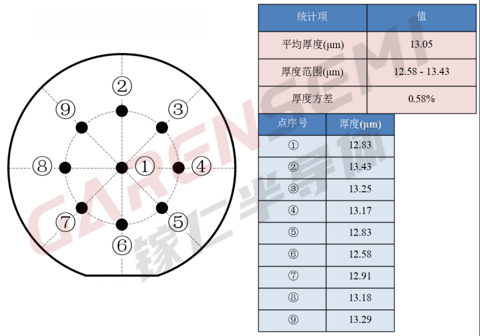
Fig.2 GAREN SEMI 8-inch epitaxial film thickness test point distribution and corresponding results
Tested via the capacitance-voltage (C-V) measurement method, the carrier concentration of the epitaxial layer ranges from 1.30×10¹⁶ cm⁻³ to 2.06×10¹⁶ cm⁻³, with an average carrier concentration of 1.79×10¹⁶ cm⁻³ and a standard deviation of 12.54%. Such superior electrical properties render the 8-inch epitaxial wafer well-suited for the fabrication of high-voltage power devices, providing high-quality material support for the subsequent R&D and mass production of related devices.
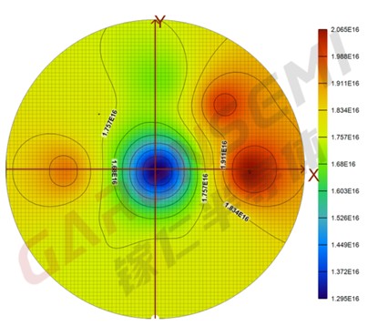
Fig.3 Carrier Concentration Distribution Cloud Map of GAREN SEMI 8-inch Epitaxial Wafer
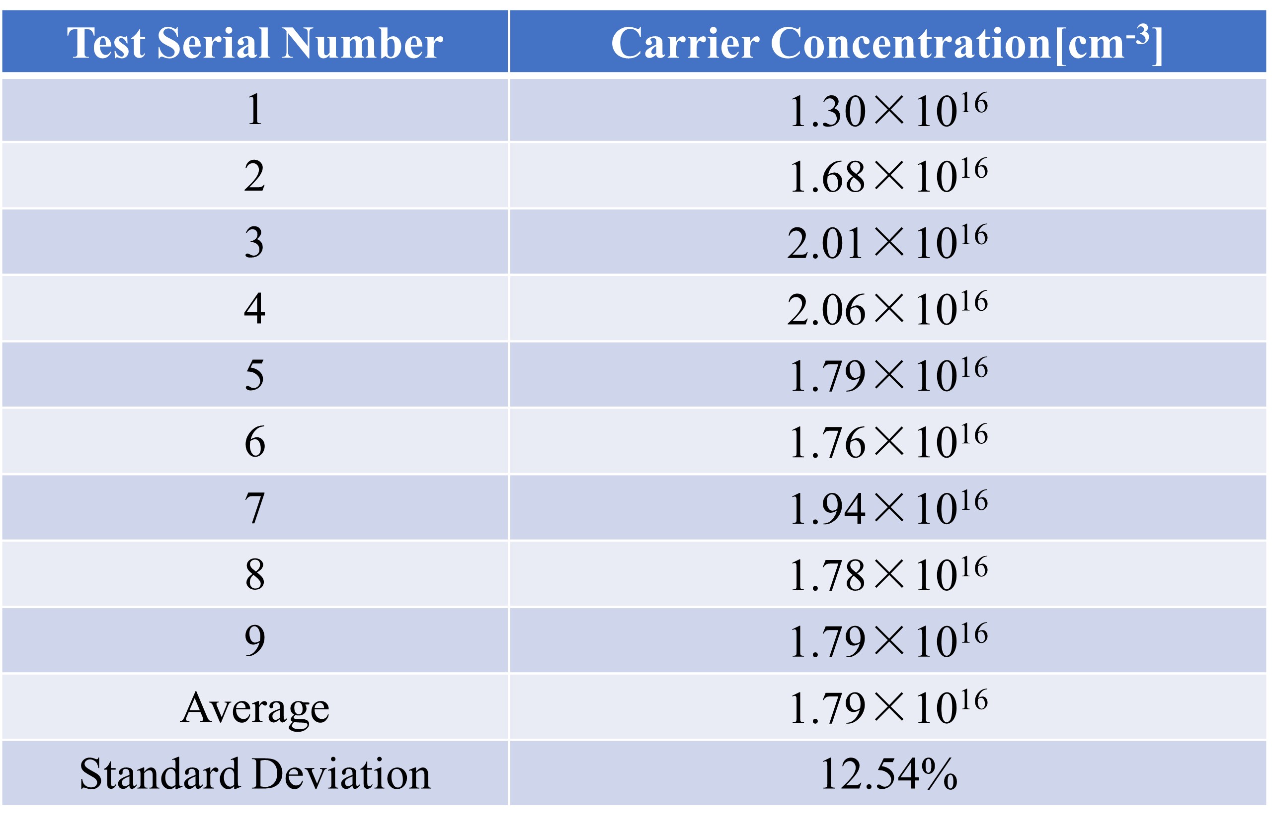
Fig.4 C-V Test Results of GAREN SEMI 8-inch Epitaxial Wafer
Gallium oxide single crystals boast a portfolio of outstanding physical properties:
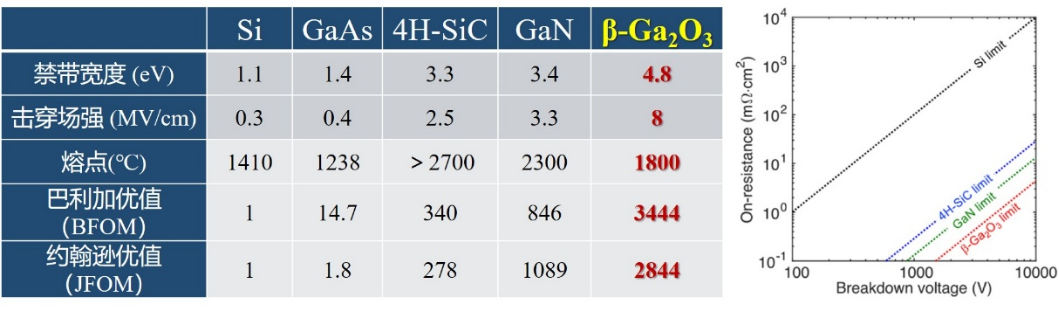
1.Its bandgap energy is approximately 4.8 eV and critical breakdown electric field around 8 MV/cm, far surpassing traditional semiconductor materials such as silicon (Si, 1.1 eV, 0.3 MV/cm), silicon carbide (SiC, 3.3 eV, 2.5 MV/cm) and gallium nitride (GaN, 3.4 eV, 3.3 MV/cm). Power devices fabricated from gallium oxide thus enable higher operating voltage and power output.
2.The Baliga's Figure of Merit (BFOM) of gallium oxide is about 10 times that of SiC and 4 times that of GaN, meaning gallium oxide-based devices feature lower specific on-resistance and higher power conversion efficiency, reducing energy loss during operation.
3.With a short ultraviolet cut-off wavelength at 260 nm, gallium oxide’s transmittance in the ultraviolet band is minimally affected by carrier concentration, endowing it with distinct advantages in the fabrication of deep ultraviolet (DUV) optoelectronic devices.
4.Additionally, gallium oxide single crystals exhibit excellent thermal stability and chemical stability, ensuring reliable operation under harsh operating conditions.
Based on its excellent physical properties, gallium oxide can support the application of high-reliability devices under extreme high voltage (device voltage resistance above 2000V), extreme power (100kW level), extreme working conditions (high radiation, wide temperature range, high humidity, long service life) and extreme environments (deep space, deep sea, deep earth, strong electromagnetic interference). Therefore, it has broad application prospects in fields such as new energy vehicles, photovoltaic energy storage, smart grids, rail transit, commercial aerospace, and 5G communication, and has great market potential.
For a long time, the difficulty in preparing large-size, high-quality epitaxial wafers has been the core bottleneck restricting the industrialization of gallium oxide. Previously, the global mainstream technology was still at the 2-4 inch level, and the homoepitaxy technology was immature, which seriously limited device cost control and large-scale application.
The breakthrough of GAREN SEMI's 8-inch gallium oxide homoepitaxial wafer will completely change the development trajectory of the gallium oxide industry from three dimensions:
1.Break the Size Bottleneck.The size of the epitaxial wafer directly determines the number of devices that can be manufactured per wafer, which is the core prerequisite for large-scale production. Compared with the current mainstream 2-4 inch epitaxial wafers, the 8-inch gallium oxide homoepitaxial wafer of GAREN SEMI can produce a larger number of power devices per wafer, which can significantly reduce the unit cost of substrate, processing, packaging and other links.
2.Solve Quality Pain Points.Homoepitaxy is the optimal path for preparing high-performance gallium oxide devices — the epitaxial layer and the substrate have perfect lattice matching, which can effectively reduce lattice mismatch and defect density, and significantly improve key performance indicators of devices such as breakdown voltage, on-resistance, and switching speed. The 8-inch homoepitaxial wafer of GAREN SEMI has excellent crystal quality and low defect density, making it possible for gallium oxide to be applied in ultra-high voltage and high-power scenarios.
3.Accelerate Industrial Upgrading.The full realization of gallium oxide's performance advantages hinges critically on the capability to produce large-size, high-quality materials. GAREN SEMI's breakthrough in 8-inch homogeneous gallium oxide epitaxial wafers not only enhances China's global competitiveness in the fourth-generation semiconductor field but will also accelerate technological iterations in the global gallium oxide industry, ushering in a new "fourth-generation" era for the global semiconductor industry.
GAREN SEMI Consolidates Global Leadership
In March 2025, GAREN SEMI successfully prepared the world's first 8-inch gallium oxide single crystal using independently developed casting method and processed the corresponding size single crystal substrate, demonstrating its technical capability in breaking through material size limits. This achievement marks that Garen Semiconductor has become the first enterprise in the world to master the 8-inch gallium oxide single crystal growth technology, setting a new global record for the size of gallium oxide single crystal.
Subsequently, GAREN SEMI completed the 8-inch gallium oxide single crystal growth by Vertical Bridgman (VB) method in just one year, becoming the world's first leading manufacturer to realize the preparation of 8-inch gallium oxide single crystals with multiple technical routes and multiple crystal planes.
The growth of 8-inch gallium oxide homoepitaxial wafers not only solves the core bottleneck of gallium oxide industrialization, but also reshapes the competitive pattern of the global gallium oxide industry. Looking to the future, Garen Semiconductor will deepen industry-university-research cooperation with universities and research institutions, attract high-end technical talents, continuously promote technological iteration, consolidate its global leading position, strive to become a global leader in gallium oxide materials and equipment solutions, and contribute core strength to the high-quality development of China's semiconductor industry.
**Contact us**
For detailed information about Garen and our products, visit http://garen.cc/ or contact:
Mr. Jiang: +86 15918719807 | jiangjiwei@garen.cc
Mr. Xia: +86 19011278792 | xianing@garen.cc
Hangzhou Gallium Semiconductors Co., Ltd. looks forward to collaborating with global partners to shape the future of semiconductor technology


官方公众号 企微客服
Copyright © 杭州镓仁半导体有限公司 2022-2023 All Rights Reserved 浙ICP备2022037154号


 技术支持
技术支持 在线咨询
在线咨询  电话联系
电话联系