
application area
晶体生长经验
Crystal Growth Expertise
打破国际垄断
China's Breakthrough in β-Ga₂O₃
知识产权积累
Invention Patents Granted
优质衬底产品
High-Quality Substrates
镓仁半导体将深耕于氧化镓上游产业链的持续创新,努力为我国的电力电子等产业的发展提供产品保障。
Garen is committed to continuous innovation across the upstream Ga₂O₃ supply chain,
providing reliable products that support the growth of the power electronics industry.
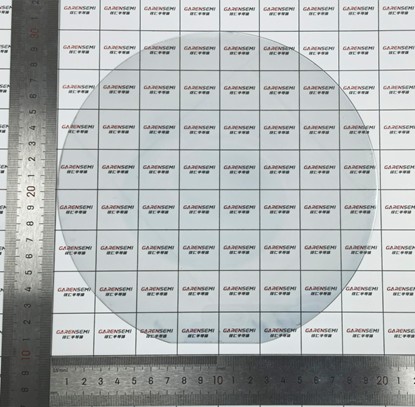

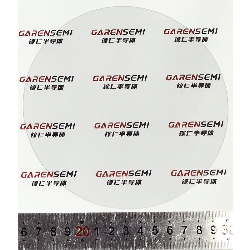
Global Premiere | The world’s first 8-inch β-Ga2O3 single crystal unveiled by Hangzhou Garen Semiconductor Co., Ltd., ushering in a new era for the fourth-generation β-Ga2O3 semiconductor
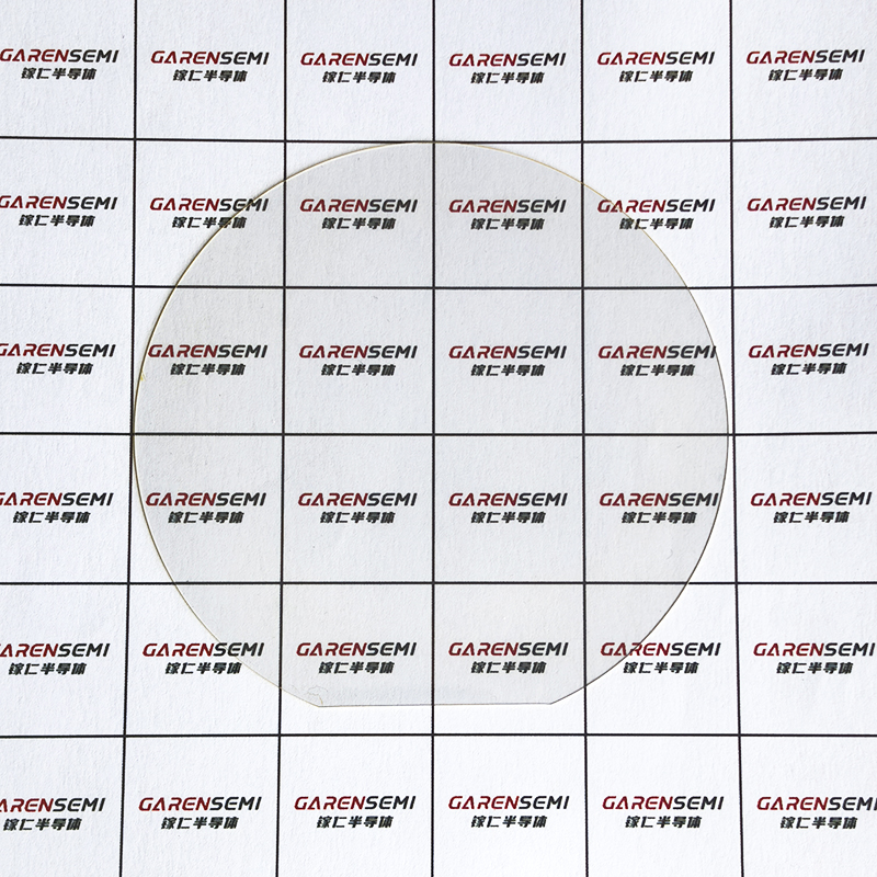
2025/03/07Hangzhou GAREN Semiconductor Co., Ltd. achieves wafer level 6-inch oblique cut gallium oxide substrate
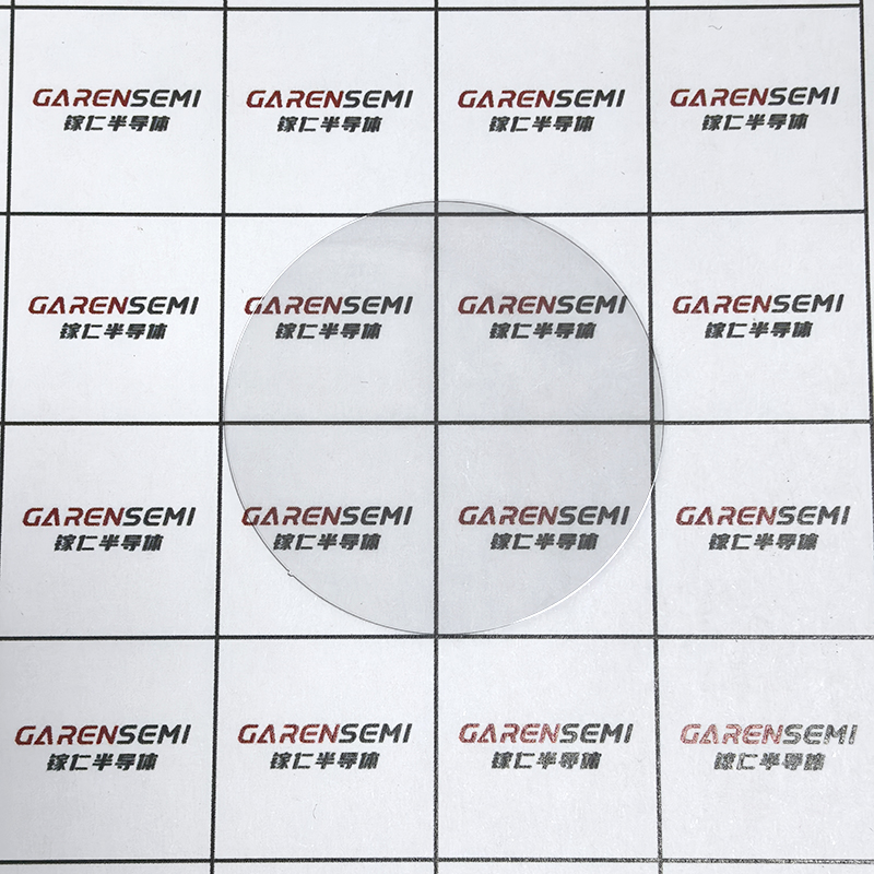
2025/07/04Global Premiere |GAREN SEMI Successfully Achieves The world’s first 8-inch Gallium Oxide Homoepitaxy
2026/03/24
官方公众号 企微客服
Copyright © 杭州镓仁半导体有限公司 2022-2023 All Rights Reserved 浙ICP备2022037154号





 技术支持
 在线咨询
 电话联系